由单片机构成的锁相环实验平台硬件设计(含任务书,开题报告,外文翻译,毕业论文14000字)
摘要:现代通信系统中,为确保通信的稳定与可靠,对通信设备的频率准确率和稳定度提出了极高的要求。传统的RC或LC信号源虽然调节方便,但是稳定性不高,而使用石英晶体振荡器虽然稳定性够高,但是它的频率调节范围又不够。采用现代锁相环频率合成器技术不仅可以使频率的调节范围达到要求,而且它的稳定性够高。所以现代锁相环频率合成技术在现在和未来的通信领域扮演重要的作用。
锁相环由鉴相器、环路滤波器和压控振荡器组成。鉴相器主要用于检测两个输入信号直接的相位之差。本次设计中相位比较器与压控振荡器VCO由锁相环LM4046 组成。1/N分频电路是一个三级可预置数分频器,各级都采用可预置数BCD码同步1/N制计数器MC14522,每级的分频比可用4 位小型拨动开关以8421BCD码形式对该级计数器进行预置数,分频比可选择的范围为0——999。当电路中输入外接信号源 后,经过电路反馈后得到压控振荡器的频率 ,电路处于锁定状态,VCO的振荡频率 =N ,改变三级程序分频器的分频比N时,VCO的振荡频率 也随着变化,同时也可以用单片机连接控制电路,通过程序驱动按键来控制分频比。这就是锁相环实现频率合成的过程。
关键词:锁相环 频率合成器 分频比
The hardware design of the PLL experimental platform based on MCU
Abstract: In order to ensure the stabilization and reliability of the communications, the modern communication systems have offered high requirements on the accuracy and stabilization in the frequency of communication equipment. Though the signal of RC or LC is adjusted conveniently, it is not steady enough. Also, the quartz crystals oscillator has a high stabilization, but the its frequency adjustment range is not enough. Using the technology of modern PLL Frequency Synthesizer, it can bring the frequency adjustment range up to the required standard and its stabilization is high enough. The technology of the modern PLL Frequency Synthesizer, takes an important part in present and future field of communication.
PLL is made up of phase detector, loop filter and voltage control oscillator. Phase detector is used by detecting the direct phase separation of the two input signals. In this design, the phase comparator and the voltage control oscillator VCO comprise PLL LM4046. 1/N scale down circuit is a three-grade frequency divider and each grade uses BCD code synchronous and 1/N counter MC14522. The input frequency of each grade gauges the initialized data base to its counter in the form of 8421BCD code, by using four small toggle switches. The optional scope of the input frequency is 0-999. When inputting the external signal generator , it received the oscillator frequency under the circuit feedback, the circuit is on the locked status, the oscillator frequency of VCO equals to N . With the changing of the input frequency N, the oscillator frequency of VCO is changing too. This is the process of frequency synthetic.
KeyWords: PLL , frequency Synthesizer, frequency dividing ratio
.
3 系统总体方案设计
用单片机实现单环式数字频率合成器构成的锁相环实验平台。具有键盘输入和显示功能,输出频率f0=1.000~999KHZ, 频率间隔1KHZ。输出电平:TTL电平。电源:+5v。通过实验设备能观察锁相环的同步过程、跟踪过程、捕捉过程,测量锁相环的同步带与捕捉带,并计算它们的带宽。能测量输入和输出信号的波形,测量并观察最小分频比和最大分频比。
3.1 系统总体硬件设计方案
实现频率合成的方法有多种,可用直接合成,锁相环式,而锁相环式的实现方法又有多种,例如可变晶振,也可变分频系数M,还可以用单片机来实现等等。本设计是采用单片机来实现频率合成,系统框图如图3.1所示。
3.1.1 锁相电路设计
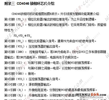
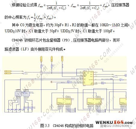
集成锁相环芯片CD4046是由CMOS电路构成的多功能单片集成锁相环,具有功耗低、输入阻抗高、电源电压范围宽等优点。在信号处理和数字系统中,CD4046都得到了广泛的应用,常被用于频率调制、频率锁定、时钟同步和频率合成等方面
目录
1 引言 1
1.1 选本课题的意义 1
1.2 锁相环的发展 1
2 锁相环与频率合成器 3
2.1锁相环的特点 3
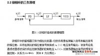
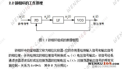
2.2锁相环的工作原理 4
2.3 锁相环的应用 8
2.4 频率合成器简介 8
2.4.1 频率合成器及其技术指标 8
2.5 频率合成器的类型 9
2.5.1 直接式频率合成器(DS) 9
2.5.2 间接式频率合成器(IS) 9
2.5.3 直接数字式频率合成器(DDS) 10
3 系统总体方案设计 11
3.1 系统总体硬件设计方案 11
3.1.1 锁相电路设计 12
3.1.2分频电路设计 15
3.1.3 单片机最小系统电路设计 18
3.1.4 键盘显示模块设计 20
3.2软件设计 23
4. 实验调试 24
4.1 锁相式数字频率合成器工作原理 24
4.2基本锁相环实验 27
4.3 锁相环频率合成器调试 28
总结 30
参考文献 31
致谢 32
附录 33
|